


- 投稿者 : FSPCBA
- 更新日: 1年以上 487 アクセス
In order to ensure that the copper surface of the solder pad on the PCB is not oxidized and polluted before soldering, the circuit boards produced by FS Technology must be protected by a surface coating (plating) layer, and the surface coating (plating) layer must meet the necessary and sufficient conditions to achieve the purpose.
Copper is second only to silver as an excellent conductor and a metal with good physical properties (such as ductility, etc.). In addition, the reserves are quite abundant and the cost is not high. Therefore, copper is selected as a conductive material for PCB. However, copper is an active metal, and its surface is easily oxidized to form an oxide layer (copper oxide and cuprous oxide). This oxide layer often causes solder joint failures and affects reliability and service life. According to statistics, 70% of the failures of FS Technology PCBs come from the solder joints. The main reasons are:
(1) It is caused by incomplete welding, virtual welding, etc. due to surface contamination and oxidation of the pad;
(2) Due to the mutual diffusion between gold and copper to form a diffusion layer or the formation of intermetallic compounds between tin and copper, failures such as interface looseness and embrittlement are caused. Therefore, the copper surface of the PCB used for soldering must be protected by a solderability protective layer or a solderability barrier layer in order to reduce or avoid failure problems.
FS Technology classifies PCB surface coating by application
1. For wire bonding: wire bonding process
Hot Air Levelling (HASL or HAL)
The method of blowing the PCB out of molten Sn/Pb solder by hot air (230℃).
2. For connectors: electroplating Ni/Au or electroless Ni/Au (hard gold, including P and Co)
3. For welding: The surface of copper must be protected by a coating layer, otherwise it will be easily oxidized in the air.
https://www.fs-pcba.com/
Corrosive
The corrosiveness of the organic heat-resistant solderability coating (plating) coating refers to the presence of corrosion on the surface of the PCB after soldering, such as corrosion on the surface of the PCB substrate and the metal layer. This is because there are more or less halides or organic acids in the organic heat-resistant solderability coating (plating) (mainly to further remove residual oxides and contaminants on copper pads), but these acidic The existence of substances after welding is harmful, in addition to decomposition and volatilization, the insufficient must be cleaned and removed.
the remains
The residue of the organic heat-resistant solderability coating (plating) coating refers to the residue on the solder pad or solder joint after the solder is soldered. Generally, these residues are harmful (such as organic acids or halides, etc.) and should be removed, so cleaning measures should be used after welding. There is no-clean soldering technology now, because the organic surface coating (plating) coating has very little post-soldering residue (most of which have been decomposed and volatilized).
FS Technology is the best circuit board company in China
heat resistance
At the high temperature of soldering, the surface coating (plating) can still protect the copper surface of the PCB pad from oxidation and allow the solder to enter the copper (or metal) surface for connection. The heat resistance of organic surface coating (plating) coating refers to its melting point and thermal decomposition (volatile) temperature performance, its melting point should be close to or slightly lower than that of solder (tin), but its thermal decomposition temperature (≥ 350°C) should be much greater than the melting point temperature and soldering temperature of the solder to ensure that the copper surface does not oxidize during soldering. The heat resistance of the metal surface coating does not have this problem.
coverage
For the organic heat-resistant solderability coating (including flux), it can completely cover the surface of the copper pad before and during the soldering process without being oxidized and contaminated, only after the molten solder is soldered to the surface of the copper pad. Swim away, decompose and volatilize, and float (cover) on the surface of the solder joint. Therefore, in order to ensure that the molten solder is completely welded on the land, the surface tension of the molten organic surface coating layer should be small and the decomposition temperature should be high, so as to ensure good coverage before and during welding. At the same time, its specific gravity is much smaller than that of molten solder (tin) to ensure that the molten solder squeezes and penetrates into the copper surface, so the coverage of the organic surface coating refers to its surface tension, specific gravity, etc. at the welding temperature performance. The metal surface coating layer is partially melted into the solder during soldering or is connected on the surface of the barrier layer.
Environmentally friendly
The environmental protection of the surface coating (plating) layer means that the waste water generated during the formation of the coating layer and the waste liquid cleaned after welding should be substances that are easy to handle, low cost and do not pollute the environment.
3. Disadvantages:
FS Technology believes that the general surface coating technology is not suitable for welding pins with fine gaps and components that are too small, because the surface flatness of the tin-sprayed board is poor. Solder beads are easily generated in PCB processing, which is more likely to cause short circuits to fine pitch components. When used in the double-sided SMT process, because the second side has undergone high temperature reflow soldering, it is very easy to re-melt the tin spray and produce tin beads or similar water droplets that are affected by gravity into spherical tin points that drop, causing the surface to be even more unsightly. Flattening in turn affects welding problems.
• The tin-spraying process once dominated the PCB surface treatment process. In the 1980s, more than three-quarters of PCBs used the tin spraying process, but the industry has been reducing the use of the tin spraying process over the past decade. It is estimated that about 25%-40% of the PCBs currently use the tin spraying process. . The tin-spray process is dirty, smelly, and dangerous, and has never been a favorite, but it's an excellent process for larger components and larger-spaced wires. In the PCB with higher density, the flatness of the tin spraying process will affect the subsequent assembly; therefore, the HDI board generally does not use the tin spraying process. With the advancement of technology, the industry has now developed a tin-spraying process suitable for QFP and BGA with smaller assembly pitch, but there are few practical applications. At present, some factories use OSP process and immersion gold process to replace tin spraying process; technological development also makes some factories adopt immersion tin and immersion silver process. Coupled with the trend of lead-free in recent years, the use of tin spraying process is further restricted. Although the so-called lead-free tin spraying has appeared at present, this may involve the compatibility of equipment.
However, the surface coating technology of FS Technology can completely avoid these shortcomings. Our technology is the most perfect at present, and we are confident that we can complete all customer needs.
その他
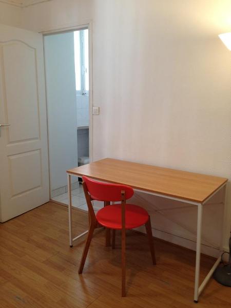
4piece
€ 2,500
9区
パリ中心部の美しく改装されたアパ
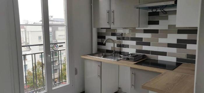
€ 1,150
13区
20m2
€ 730
13区
52m2
€ 1,500

初級・初心者のための1対1オンライン教室「はじめてフランス語 ..

こんにちは。 日本の国家資格「柔道整復師」を取得後、スポー ..